3D TCAD FINFET Models

An interesting project from the IuE Summer of Code 2014 is a collection of 3D CAD models. On the CAD models page are examples of these devices.

  • MOSFET and Single-Gate
  • Double-Gate
  • Tri Gate
  • All-Around-Gate
  • FlexFET
  • Special Gate-Form Devices

Using the FreeCAD open source CAD modeling software. The student created these models from examples in the literature. There are also tutorials at the bottom of the page for building a Double-Gate MOSFET and Tri-Gate devices.

2dmatter.com

The NanoTCAD ViDES team has announced their new website, http://www.2dmatter.com.

From their announcement:

The website is intended to be a useful tool in order to link to all the recent publications concerned with Two-dimensional materials from the main journals in the field, i.e., (up to now) Physical Review Letters, Physical Review B, Applied Physics Letters, IEEE Transaction on Electron Devices, IEEE Electron Device Letters, IEEE Nanotechnology, Proceedings of IEEE, Scientific Reports, Nature Nanotechnology, ACS NANO and Nano Letters.

TCAD Software Job

Sandia National Labs is looking for a TCAD software engineer who is a US citizen and is able to get a security clearance.  From their description:

We have an immediate technical staff opening for a semiconductor device modeling software developer with expertise in scientific programming for high performance computing.  The position emphasizes algorithm design and enhancement to extend the capabilities and increase the efficiency of our large scale, parallel, drift-diffusion solver, which is a C++/object oriented program.  The successful candidate will be part of a team of computational scientists and semiconductor device physicists.  Additionally, the position requires extensive interaction with experimental and theoretical physicists and research engineers working on characterizing radiation effects in microelectronic devices and the resulting changes to circuit performance.

I was aware that they had a software named Charon, which leveraged a commercial tool. It looks like they may be developing their own replacement. A quick google search revealed a mailing list for their git archives of the tool. It appears the tool has been in development at least since January 2012.

Fujitsu Simulates Graphene Device Using Open Source Tool

Fujitsu announced the simulation of a 3030 Atom Nano device here on January 14th, 2013. The simulation took 20 hours on their supercomputer to simulate the electrical properties of graphene and an insulating layer, using OpenMX Material Explorer.

Even more interesting is the news that OpenMX is an open source tool available from openmx-square.org under the terms of the GPL.

Aestimo version 0.9

Sefer Bora Lişesivdin announced the release of Aestimo GPL 1D Schrödinger-Poisson solver last month. From his announcement on LinkedIn:

Aestimo Team is proud to release the version 0.9 of Aestimo 1D Self-consistent Schrödinger-Poisson Solver. This version includes many bugfixes, speed improvements, cython code additions, rewritten VBMAT-V part to use numpy better, merging conduction and valance band calculations and more. Code is heavily modified and stabilized.

The software is available for download from: https://bitbucket.org/sblisesivdin/aestimo/downloads.

Welcome

This blog focuses on both EDA and TCAD software.  From time to time I’ll be posting about these topics and hope that you find these useful.

DEVSIM is now Open Source

DEVSIM is now open source. The core engine is licensed under the LGPL 3.0 license, meaning it is available for use in your own software. The project home page is here:

https://devsim.org

The direct link to the documentation is here:

https://devsim.org/manual

I hope that this software is useful to the TCAD simulation community. Please let me know if you have any questions about installation or usage of the software.

1D diode junction, part II

In the previous blog post, 1D diode junction I showed some simulation results, here I share some of the actual script for the physics behind this example.

For the poisson equation, the implementation is:

pne = "-ElectronCharge*kahan3(Holes, -Electrons, NetDoping)"
CreateNodeModel(device, region, "PotentialNodeCharge", pne)
CreateNodeModelDerivative(device, region, "PotentialNodeCharge", pne, "Electrons")
CreateNodeModelDerivative(device, region, "PotentialNodeCharge", pne, "Holes")


equation(device=device, region=region, name="PotentialEquation", variable_name="Potential",
node_model="PotentialNodeCharge", edge_model="PotentialEdgeFlux",
time_node_model="", variable_update="log_damp")

where “PotentialEdgeFlux” was defined elsewhere in the script as “Permittivity * ElectricField”. The “kahan3” function is provided to add 3 numbers with additional precision.

For the electron and hole current densities, the Scharfetter-Gummel method is used to calculated the current along each edge connecting the nodes in the mesh. The Bernoulli function, B(x) and its derivative, dBdx(x) are provided in the DEVSIM interpreter

vdiffstr="(Potential@n0 - Potential@n1)/V_t"
CreateEdgeModel(device, region, "vdiff", vdiffstr)
CreateEdgeModel(device, region, "vdiff:Potential@n0", "V_t^(-1)")
CreateEdgeModel(device, region, "vdiff:Potential@n1", "-vdiff:Potential@n0")
CreateEdgeModel(device, region, "Bern01", "B(vdiff)")
CreateEdgeModel(device, region, "Bern01:Potential@n0", "dBdx(vdiff) * vdiff:Potential@n0")
CreateEdgeModel(device, region, "Bern01:Potential@n1", "-Bern01:Potential@n0")
Jn = "ElectronCharge*mu_n*EdgeInverseLength*V_t*kahan3(Electrons@n1*Bern01, Electrons@n1*vdiff, -Electrons@n0*Bern01)"
CreateEdgeModel(device, region, "ElectronCurrent", Jn)
for i in ("Electrons", "Potential", "Holes"):
  CreateEdgeModelDerivatives(device, region, "ElectronCurrent", Jn, i)

In this example, the @n0, and @n1 refers to the variables on each node of the edge. For an edgemodel, “foo”, a derivative with respect to variable on the first node, “bar”, would be “foo:bar@n0”.

For the Shockley Read Hall recombination model, the implementation is:

USRH="(Electrons*Holes - n_i^2)/(taup*(Electrons + n1) + taun*(Holes + p1))"
Gn = "-ElectronCharge * USRH"
Gp = "+ElectronCharge * USRH"
CreateNodeModel(device, region, "USRH", USRH)
CreateNodeModel(device, region, "ElectronGeneration", Gn)
CreateNodeModel(device, region, "HoleGeneration", Gp)
for i in ("Electrons", "Holes"):
  CreateNodeModelDerivative(device, region, "USRH", USRH, i)
  CreateNodeModelDerivative(device, region, "ElectronGeneration", Gn, i)
  CreateNodeModelDerivative(device, region, "HoleGeneration", Gp, i)

The purpose of this post is to describe some of the physics used in the previous example, and show how they are implemented within the DEVSIM software using a scripting interface. Once a set of physical equations has been implemented, it can be placed in modules that can be reused for other simulations.
1D diode junction

It’s always nice when you can get a textbook result from your simulator.

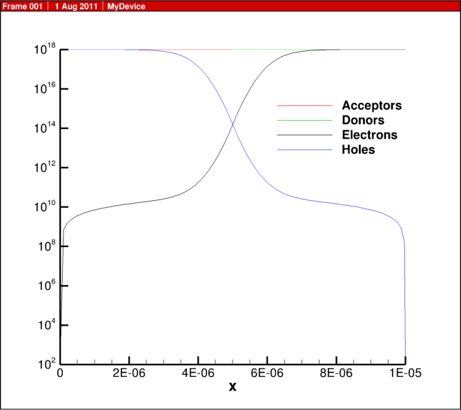
This is the doping profile, and the resulting carrier densities for a forward bias of 0.5 V.

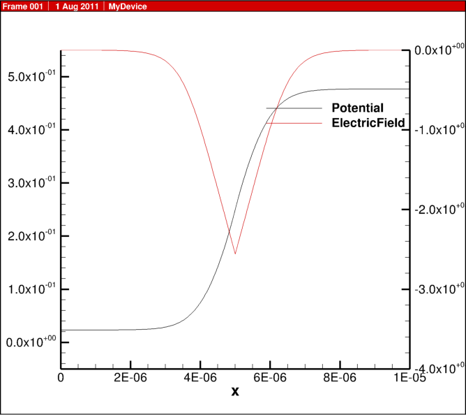
The potential and electric field.

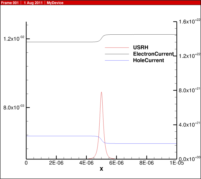
The electron and hole current densities and SRH recombination.